PCB layout
A good schematic does not guarantee a working board. The layout decides whether the board passes EMC, whether it overheats, and whether the factory can build it without surprises. We lay out the PCB with a full understanding of the circuit, because we also designed it and write the code that runs on it.
What we do
- Multi-layer boards and stack-up design
- Impedance control for high-speed lines and differential pairs
- RF and antenna layout
- Flex and Rigid-Flex
- High-power boards: copper width, heat spreading and isolation clearances
- EMC/EMI design from the layout stage
- DFM and DFT: design for manufacturing and testing
When to call us
- You have a schematic and need a professional layout
- The board failed EMC testing
- The board must shrink or fit an existing enclosure
- The factory keeps sending manufacturing comments on the board
What you get
- Gerber and ODB++ files
- Pick & place and drill files
- Assembly drawing and stack-up for the factory
- Project source files
FAQ
Which EDA tools do you use?
KiCad and Altium Designer. We can also work in your team's tool, so you can maintain the project yourselves.
Do you also order manufacturing?
Yes, if you want. We work with PCB and assembly houses in Israel and abroad and support the first prototype batch. We are not a PCB factory ourselves.
// Projects
Examples from the field
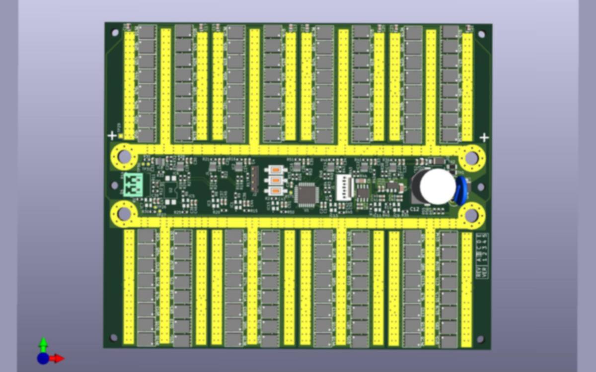
Industrial · High power
Multi-channel spot-welding controller
- Challenge
- Deliver pulses of up to 1500 A with precise timing, without burning parts on every pulse.
1500AMaximum pulse current
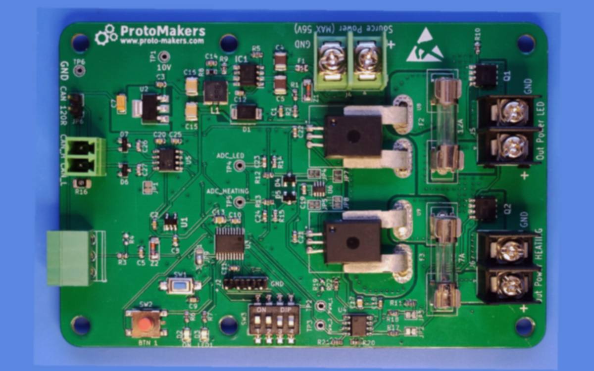
Industrial · Power · CAN
Power management board with CAN
- Challenge
- Control two heavy loads, lighting and heating, from an input of up to 56 V, and protect the board from short circuits and overload.
56VMaximum input voltage
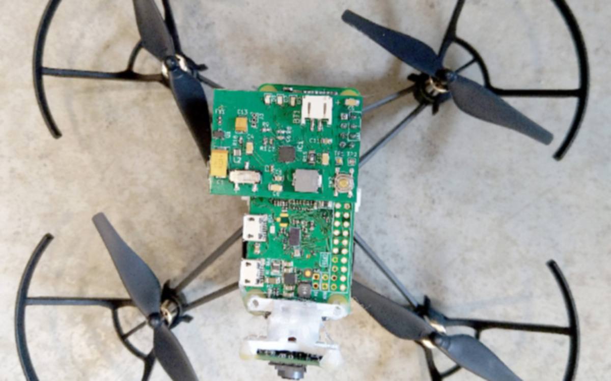
Robotics · Real time
Drone with a custom PCB
- Challenge
- A light, compact board that combines motor control, sensors and wireless communication, without noise that disturbs the sensors.
Real-timePrecise wireless control
Have a project on the table?
A free 30-minute intro call, no obligation.